DIODA poza MOSfetem... (freeweeling diode)
a teraz rozważmy TĘ drugą diodę którą należałoby umieścić samodzielnie...

pare słówek
o chopperze..
Free Wheeling Diode
The free wheeling diode has a unique function in the circuit. It ensures that the output voltage during each "off" time, allotted by the MOSFET, is equal to 0 V. It achieves this by acting as a sink for the motors internal inductance. That is, when the MOSFET stops conducting, the current stored in the motor's inductance discharges itself through the motor and the diode. The observed effect is that the motor continues operation despite drawing no current from the battery.
...następny temat istotny to "The Snubber Circuit".... cdn... czyli JAK NIE SIAĆ ZANADTO!!!
albo inaczej => ElectroMagnetic Compatability
bo przy kluczowaniu indukcyjności bez środków zaradczych złamiemy CE

The Snubber Circuit
Much of the power lost when using transistors is due to switching. Snubber circuits reduce power losses in transistors during switching and protect them from the switching stresses of high voltages and currents. Switching contributes to a large amount of the power lost when using transistors. Therefore, to conserve energy in our circuit it was a good idea to implement a snubber circuit into our design. The figure below displays the snubber configuration that we used and a simplified version of the rest of the DC chopper.

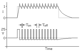
Consider the above figure without the snubber circuit addition. When the transistor is operating in the on state, the diode D1 is off, and the MOSFET is carrying the load current. As the transistor turns off, the diode remains reverse biased until the transistor voltage Vm, is equal to the source voltage Vs and the load voltage Vl decreases to 0 V. When the transistor voltage reaches Vs, Id increases to Il and the diode begins to conduct while the MOSFET current decreases to zero. During this operation there is a region where the MOSFET has a current going through it and a voltage across it. Therefore there is a power loss spike as shown in the figure below. A similar effect occurs when the MOSFET is turned on again. There is a build up of voltage and a flow of current simultaneously. These power loss spikes are undesirable and a snubber circuit helps lessen their impacts.

One purpose of the snubber circuit is to alter the voltage and current waveforms produced during switching to an advantage. With our snubber circuit invoked there is another path for the load current during turn-off and the capacitor in it reduces the rate of change of the MOSFET voltage. It delays the voltage transition from low to high. The capacitor charges to the MOSFET off-state voltage Vm, and remains charged until the MOSFET turns on again. The figure below displays the resulting waveforms and the power loss spike.

Because the voltage and current levels exist at varying degrees of magnitude, the resulting power loss can be configured so it is a lot lower than normal operation. The size of the capacitor determines the rate at which the voltage changes across the MOSFET at turn-off. There is also a resistance in the snubber circuit. The resistance is chosen such that the capacitor is discharged before the next time the MOSFET turns on. Care is required when selecting the values of capacitance and resistance are to be implanted in a circuit. A large capacitor reduces the power loss in the transistor, but in turn it increases the amount of power lost in the snubber resistor. If designed properly a snubber circuit can reduce the total switching losses, but the most important result is that it reduces the losses in the MOSFET itself which in turn reduces its cooling requirements. This is very important because MOSFET's are quite susceptible to temperature variations and are much harder to cool than resistors. Therefore, the snubber makes the entire design much more reliable.
...
strona o
EMC - ElectroMagnetic Compatability
[ Dodałem: 2004-10-12, 13:25 ]
2.3. Snubber networks
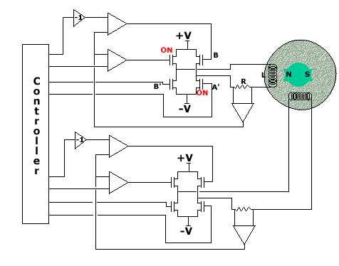
Snubber networks are combinations of resistors and capacitors that are connected across either the source of electrical noise spikes, or across the component (switch or MOSFET) to be protected from those spikes, or maybe both. The diagram below shows a motor load with resistance and inductance, with a snubber network fitted across (a) the motor contacts, and (b) the MOSFET. RN and CN are the resistance and capacitance of the snubber network, and RL and L are the resistance and inductance of the motor. The MOSFET is shown as a simple switch.

The RC network has several effects:
- -It reduces the voltage that is generated across the MOSFET by the inductance of the motor. To reduce this to less than Vmax volts requires that CN > L×(IL/Vmax)2 where IL is the load current.
-It reduces the rate of voltage change. To reduce this to less than 1 Volt per microsecond requires that CN > ILx10-6.
Inductors do not instantly "let go" of a current. At the instant the MOSFET truns off, the current through the MOSFET does not want to change. Using Ohm's Law (V = IR), we can see that when the MOSFET is turned on, the resistance is essentially zero, making the voltage zero as well. As the MOSFET truns off the resistance begins to increase. This leads to the generation of a high voltage which is generally destructive to the MOSFET.
Capacitors will restrict an instantaneous change in voltage. A capacitor, therefore, is useful to counter the destructive voltages generated across the MOSFET. When the MOSFET is on, the capacitor is out of the circuit (it is shorted out). As the MOSFET is turned off any change in voltage is restricted by the capacitor.
A capacitor alone is not an ideal solution. When the MOSFET is off, the capacitor charges up to the battery voltage. As the MOSFET turns on, an inrush of current results as the capacitor discharges, limited only by a MOSFET on-resistance and capacitor series resistance, and damage may still result. For this reason, a resistor is configured in series with the capacitor. The higher the resistance value, the smaller the inrush current but the less effective is the capacitor.
An Acrobat document describing the design of snubber networks is available
here here, although this is rather technical. Snubbers can be bought off-the-shelf from general electronic suppliers. Some manufacturers of snubbers are listed in the links section at the bottom of this page.
For more details on snubber network design, there is a new page devoted to the subject
here.
...
linki o snubberze:
[ Dodano: 2004-10-15, 12:13 ]
Jeszcze o SNUBBERZE
Na stronie
http://elektro.w.interia.pl/faq/09.html odnalazłem bardzo pasujące do tematu wyjaśnienie zagadnienie - i to "po naszemu"...

a to wykres ilustrujący te "momenty" strat energii(ciepła) w których ulega podgrzaniu nasz przełączający klucz...
tak może wyglądać ukłan snubbera (układ odciążający)

Dochodzimy tak do wad układu: ograniczenie maksymalnej częstotliwości przełączania (przez stałą RC); a ponadto kondensator rozładowuje się poprzez klucz (powiększenie strat przewodzenia).
Podsumowanie. Najczęściej stosuje się układy RDC (jak wyżej zaznaczono straty wyłączania są zazwyczaj większe od strat włączania). Najlepiej jednak wogóle unikać stosowania sieci jeśli jest to tylko możliwe (np. w elementach o bardzo krótkich czasach przełączania). Układy te ograniczają zakres regulacji (ograniczenie częstotliwości przełączania) oraz komplikują układ (dodatkowe koszty).


")


")

")